產品介紹
-
-
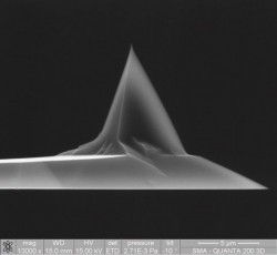
Conductive tip coating with PtIr / TiN / Au
Our standard silicon probes are available with conductive coatings – Au, TiN, PtIr. Extremely sharp tips allow the user to obtain high-quality images of samples. Standard chip sizes make our probes compatible with most AFM manufacturers.
產品說明
Specifications
| Cantilever | Length | Width | Thickness | Resonant Frequency kH z | Force Constant Nm | |||||
|---|---|---|---|---|---|---|---|---|---|---|
| ± 10μm | ± 5μm | ± 0.5μm | min | typical | max | min | typical | max | ||
| NSG01 | 125 | 30 | 2 | 87 | 150 | 230 | 1.45 | 5.1 | 15.1 | |
| NSG03 | 135 | 30 | 1.5 | 47 | 90 | 150 | 0.35 | 1.74 | 6.1 | |
| NSG10 | 95 | 30 | 2 | 140 | 240 | 390 | 3.1 | 11.8 | 37.6 | |
| NSG30 | 125 | 40 | 4 | 240 | 320 | 440 | 22 | 40 | 100 | |
| CSG01 | 350 | 30 | 1 | 4 | 9.8 | 17 | 0.003 | 0.03 | 0.13 | |
| CSG10 | 225 | 30 | 1 | 8 | 22 | 39 | 0.01 | 0.11 | 0.5 | |
| CSG30 | 190 | 30 | 1.5 | 26 | 48 | 76 | 0.13 | 0.6 | 2 | |
| FMG01 | 225 | 32 | 2.5 | 40 | 60 | 96 | 1 | 3 | 5 | |
Cantilever Specifications
| Material | Single Crystal Silicon, N-type, 0.01-0.025 Ω-cm, Antimony doped |
| Cantilever Geometry | Rectangular (cross-section is trapezium) |
| Back Side Coating | Au, TiN, or PtIr |
| Tip Side Coating | Au, TiN, or PtIr |
| Coating Thickness | Au: 35nm TiN, PtIr: 25nm |
Tip Specifications
| Tip Geometry | Tetrahedral, the last 500 nm from tip apex is cylindrical |
| Tip Height | 14 – 16 μm |
| Tip Aspect Ratio | 3:1 – 7:1 |
| Tip Offset (Setback) | 5 – 20 μm |
| Tip Front Angle | 10 ± 2° |
| Tip Back Angle | 30 ± 2° |
| Tip Side Angle (half) | 18 ± 2° |
| Tip Cone Angle | 7 – 10° |
| Tip Curvature Radius (Nom) | 20 nm |
| Tip Curvature Radius (Max) | 35 nm (guaranteed) |
General Information
> Standard chip size: 1.6×3.4×0.3 mm> The base silicon is highly doped to avoid electrostatic charges.